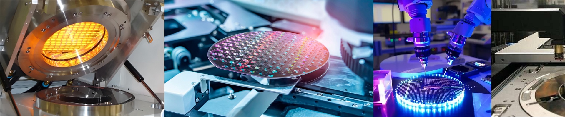
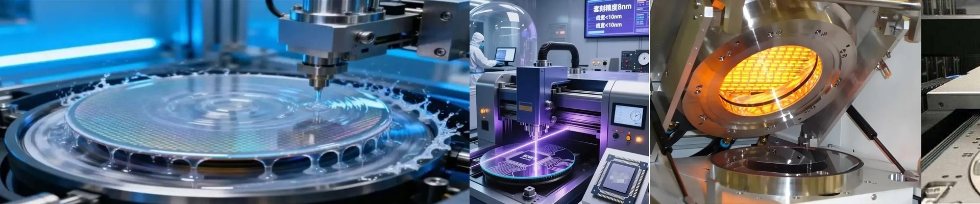

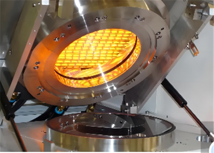
Right before packaging, any moisture left behind after cleaning doesn’t just sit there—it can migrate into the encapsulant. That shifts the CTE and sets you up for delamination down the line. And if you’re still running conventional hotplates, you know the drill: edge bead is a constant fight, and particle generation is a headache you can’t afford. You need drying and photoresist thermal steps that are clean, repeatable, and thermally tight. What actually matters on the floor We lean on short-wave NIR with quartz emitters, tuned to the water and solvent absorption bands. It drives sub-surface heating fast, without scorching organics. Across the active surface, wafer-level uniformity holds at ±0.1°C, and setpoint ramps are controlled within ±0.5°C/s. The platform fits Class 1–100 cleanrooms, and we can verify zero particle generation below 0.1 μm at 0.35 μm/min. Soft bake and hard bake profiles stay repeatable lot to lot, so critical dimension control stays in spec. Why this plays well in pre-packaging In pre-packaging fab, the flow is straightforward: wafer drying, then photoresist processing and curing. NIR cuts the thermal budget, shortens bake time, and trims energy draw. The payoff is faster cycles, less carryover moisture, and fewer rejects from edge bead or residual solvent. Since the same platform handles both drying and bake steps, validation gets simpler and spare parts stay lean. The things you learn the hard way NIR is line-of-sight, so you need reflective fixtures and proper wafer orientation to keep uniformity where you want it. Emitter spacing and power density have to match your wafer size and film stack, so we work up the recipe together. Plan on a short commissioning run to dial in ramp rates and dwell times. Once that’s set, the process runs with minimal drift.